
 +1 631-425-0938
 Contact
 Search
 C.A.P. Product Lookup
 Translate
PPI 0201BB103BB – Horizontal or Vertical Orientation
PPI 0201BB103 6.6mil Rogers 4350B Substrate: Scattering Matrix Measurement Conditions and Notes
This describes the considerations and measurement conditions used in the creation of the PPI 0201BB103 capacitor scattering matrix, where the sample was mounted on a 6.6mil Rogers 4350B substrate. All comments apply to a part in a series configuration , i.e. a capacitor that spans a gap in the center trace of a microstrip transmission line.
Scattering parameters of multilayer ceramic capacitors mounted on microstrip substrates depend not only on the dielectric and electrode capacitor structure, but on a number of substrate-related parameters. These include: (1) substrate dielectric constant and thickness; (2) mounting pad and trace dimensions; and (3) capacitor orientation (internal electrode planes relative to the substrate surface), horizontal or vertical.
Measurements were made for the 0201BB103 by PPI. The measurements employed coplanar probes and coplanar-to-microstrip transitions; these, as well as any other structures between the probes and the capacitor-under-test mounting pad edges, were de-embedded using statistical TRL techniques. Tests were performed on a Vector Network Analyzer from 0.4 to 32 GHz.
The scattering matrix is simply a text file; an example is shown below:
# MHz S dB R 50
400 -8.756 -70.431 -0.626 19.472 -0.626 19.472 -8.756 -70.431
410 -8.939 -70.943 -0.599 18.956 -0.599 18.956 -8.939 -70.943
420 -9.119 -71.436 -0.573 18.46 -0.573 18.46 -9.119 -71.436
430 -9.295 -71.91 -0.549 17.982 -0.549 17.982 -9.295 -71.91
440 -9.468 -72.366 -0.527 17.522 -0.527 17.522 -9.468 -72.366
450 -9.638 -72.806 -0.506 17.078 -0.506 17.078 -9.638 -72.806
The first line is a header, designated by the “#” character. Succeeding characters describe respectively the frequency units, parameter, measurement format, and characteristic impedance of the measurement system in Ohms. (Note: for the BB series, the frequency unit is Hertz, not MHz, and the measurement format is magnitude-angle, rather than dB magnitude angle shown in the example.) The data is arranged as follows: The first column is the frequency, in the units specified in the header. The next two columns are S11 magnitude (again, as specified in the header) and S11 phase. Succeeding column pairs represent S21, S12, and S22.
It should be noted that some software simulators may require that artificial data — e.g. 0 dB return losses and very large insertion losses — be added at zero frequency to avoid passivity or other issues. In general, caution is suggested when using software simulation, since many programs attempt to extrapolate scattering matrix data both below and above the frequencies where it is valid – and often arrive at grossly incorrect results. Parallel resonances in the series microstrip configuration manifest as notches (“suckouts”) in S21 or S12, the insertion loss.
Fig. 1 depicts the 0201BB103 on the mounting pads of the test substrate.
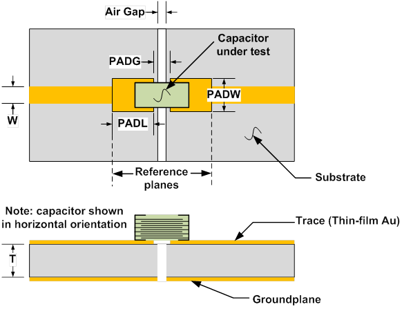
Fig. 1 The PPI 0201BB103 capacitor on the test substrate
Reference planes are always at the pad edges, as shown. The following parameters apply:
Series: 0201BB103
Part Orientation: Horizontal or Vertical
Substrate: Rogers 4350B
Substrate dielectric constant: 3.66
Substrate thickness (mils): 6.6
PADG (mils): 3
PADL (mils): 8.5
PADW (mils): 13
50-Ohm Trace Width on substrate (mils): 13
Reference plane spacing (mils): 20.0
The last two parameters, “50-Ohm Trace Width on substrate (mils)” and “Reference plane spacing (mils)” are for reference only. To determine the intrinsic properties and capabilities of a part, it is often valuable to characterize it with minimal exogenous parasitics, in this case, the fewest additional parasitic reactances beyond those of the basic capacitor spanning a gap in a microstrip trace. Generally, two conditions are necessary to accomplish this:
- Mounting pad dimensions that conform to those of the terminations on the part. (Note that most of the time this condition will not be practical in large-scale manufacturing, where mounting pads must be larger than part terminations to accommodate dimensional and placement tolerances and create room for solder fillets.)
- A 50-Ohm characteristic impedance trace width close to the part width. This (a) avoids the discontinuities created by large width disparities; and (b), for DC blocking applications where the series capacitive reactance and ESR can be neglected, creates a per-unit-length series inductance and shunt capacitance close to that of a 50-Ohm line. Fig. 2 illustrates how the general equivalent circuit for a multi-layer ceramic capacitor on microstrip approximately reduces, for a DC blocking application, to the lumped equivalent circuit for a short length of transmission line.
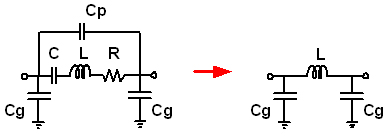
Fig. 2 General equivalent circuit for MLCC on microstrip (left) approximately reduces, for DC block, to lumped equivalent circuit for short length of transmission line (right)
PPI has created at least one set of scattering matrices in each series where the reference planes closely coincide with the nominal part edges, and where the 50-Ohm trace width on a particular substrate is close to the nominal part width. Mounting pad dimensional limitations in the models determined to what degree these conditions could be achieved.
DISCLAIMER: Passive Plus (PPI) has made every effort to make this information as accurate as possible. However, no responsibility is assumed by PPI for its use or for any infringements of rights of third parties that may result from its use. PPI reserves the right to revise the content or modify its product line without prior notice.
Capacitor Application Program
A simulation/selection web-based software tool, for engineering ease of use and critical decision making.
